2.Jiangxi Copper Technology Institute Co.,Ltd.,Nanchang330096,China
Citations
YU Mengshi,HU Siqi,HUAI Yangyang. Recent progress on preparation of cadmium zinc telluride thin films [J]. Copper Engineering,2026(1):1-18.
Abstract
Cadmium zinc telluride (CdZnTe) thin films, characterized by a high atomic number, tunable optical bandgap, and excellent photoelectric conversion performance, hold significant potential in advanced applications such as thin-film photovoltaic cells, infrared imaging, and high-energy radiation detection. However, achieving low-cost fabrication and high-quality film formation remains a critical challenge for their industrial deployment. In this work, we systematically reviewed the vapor deposition techniques for CdZnTe thin films. While methods such as physical vapor transport, vacuum thermal evaporation, hot-wall epitaxy, magnetron sputtering, and close spaced sublimation offer advantages in simplicity and cost-effectiveness, they suffer from issues such as poor film uniformity and high lattice defect density. In contrast, molecular beam epitaxy and metal-organic chemical vapor deposition enable atomic-level precision and superior lattice integrity, but are constrained by high process costs and complex equipment, limiting their scalability. To enhance the quality of CdZnTe thin films, this work highlighted three key optimization strategies: (1) refining growth parameters for precise process control, (2) improving heteroepitaxial quality through interfacial buffer layer design, and (3) mitigating intrinsic defects via annealing treatments. Ultimately, we concluded that balancing film performance with production costs and overcoming the technical challenges of large-area uniform film deposition would be critical for the future advancement of CdZnTe thin films.
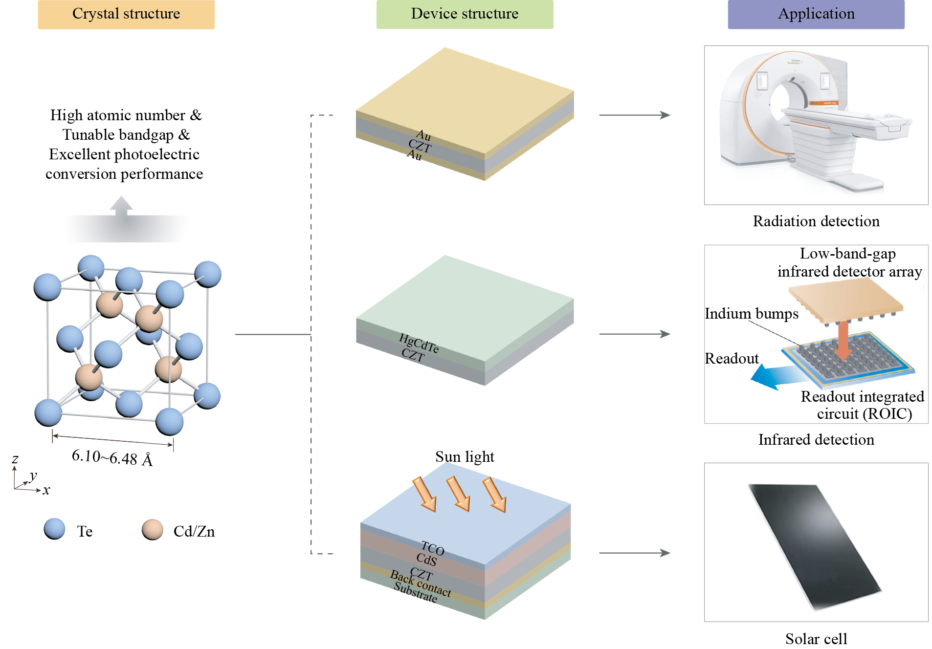
碲锌镉(cadmium zinc telluride,CZT)是一种新型化合物半导体材料,可通过Zn掺杂CdTe而成,其化学通式为Cd1-xZnxTe(0<x<1)。如图1所示,CZT晶体属于F3m空间群,具有典型的闪锌矿结构,可视为由两种亚晶格嵌套构成:Te原子占据面心立方格点的Te亚晶格,Cd和Zn原子随机占据面心立方格点的Cd/Zn亚晶格,两者沿体对角线方向相对位移1/4晶格长度。通过调控Zn元素的掺杂浓度(x值),可实现禁带宽度、载流子迁移率等性质的连续调控。这种优异的可调特性使CZT材料在以下三大前沿领域得到重要应用:作为薄膜光伏电池中光吸收层材料[ CHANDER S,DE A K,DHAKA M S. Towards CdZnTe solar cells:an evolution to post-treatment annealing atmosphere[J]. Solar Energy,2018,174:757-761. BASHIR K,MEHBOOB N,ALI A,et al. Fabrication and characterization of Cd1-xZnxTe thin films for photovoltaic applications[J]. Materials Letters,2021,304:130737. SHARMA R,CHUHADIYA S,KAMLESH,et al. CdZnTe thin films as proficient absorber layer candidates in solar cell devices:a review[J]. Energy Advances,2023,2(12):1980-2005. 1-3]、红外探测器的外延衬底材料[ REDDY M,PETERSON J M,LOFGREEN D D,et al. MBE growth of HgCdTe on large-area Si and CdZnTe wafers for SWIR,MWIR and LWIR detection[J]. Journal of Electronic Materials,2008,37(9):1274-1282. REDDY M,PETERSON J M,VANG T,et al. Molecular beam epitaxy growth of HgCdTe on large-area Si and CdZnTe substrates[J]. Journal of Electronic Materials,2011,40(8):1706-1716. TSYBRII Z,BEZSMOLNYY Y,SVEZHENTSOVA K,et al. HgCdTe/CdZnTe LPE epitaxial layers:from material growth to applications in devices[J]. Journal of Crystal Growth,2020,529:125295. 4-6]以及高能射线探测材料[ NAN R H,WANG P F,JIAN Z Y,et al. Investigation on electrical transport properties of CdZnTe pixel detector[J]. Acta Physica Sinica,2017,66(20):206101. ABBENE L,PRINCIPATO F,GERARDI G,et al. Room-temperature X-ray response of cadmium-zinc-telluride pixel detectors grown by the vertical bridgman technique[J]. Journal of Synchrotron Radiation,2020,27(2):319-328. MCCOY J J,KAKKIRENI S,GILVEY Z H,et al. Overcoming mobility lifetime product limitations in vertical bridgman production of cadmium zinc telluride detectors[J]. Journal of Electronic Materials,2019,48(7):4226-4234. LI Z W,CHENG J X,LIU F,et al. Research on the technological progress of CZT array detectors[J]. Sensors,2024,24(3):725. 7-10]。
图1 碲锌镉的晶体结构与应用领域
Fig. 1 Crystal structure and applications of CZT
在薄膜光伏电池领域中,目前以CdTe多晶薄膜为核心的光伏技术已在产业化层面验证了其经济性与可靠性。1.45 eV的准直接带隙使其与太阳光谱高度匹配,结合超过105 cm−1的光吸收系数,其单结器件的光电转换理论极限效率达32%,显著优于传统硅基技术[ BASHIR K,MEHBOOB N,ALI A,et al. Fabrication and characterization of Cd1-xZnxTe thin films for photovoltaic applications[J]. Materials Letters,2021,304:130737. 2]。产业化进程方面,从首个CdTe光伏器件诞生至今,实验室单片效率已突破22%里程碑,量产组件效率稳定在18%~20%区间,占据全球薄膜光伏市场主导地位。CZT作为CdTe经Zn元素掺杂调控的性能升级材料,可为构建高效叠层电池提供理想解决方案。CZT薄膜与窄带隙钙钛矿或晶硅形成异质结时,有望突破单结电池的转换效率极限,理论模型显示其转换效率可突破45%阈值[ SHARMA R,CHUHADIYA S,KAMLESH,et al. CdZnTe thin films as proficient absorber layer candidates in solar cell devices:a review[J]. Energy Advances,2023,2(12):1980-2005. 3]。
在红外探测成像领域,CZT材料展现出独特的工程应用价值。以碲镉汞(HgCdTe)红外焦平面探测器为例,其核心性能瓶颈在于异质外延过程中衬底与功能层的晶格适配性。CZT材料具有组分可调性优势,通过调节Zn/Cd比例,可实现与HgCdTe外延层的完美晶格匹配(失配度<0.3%)[ REDDY M,PETERSON J M,LOFGREEN D D,et al. MBE growth of HgCdTe on large-area Si and CdZnTe wafers for SWIR,MWIR and LWIR detection[J]. Journal of Electronic Materials,2008,37(9):1274-1282. 4]。此外,CZT衬底的宽带隙特性可有效抑制载流子隧穿效应,其高介电常数(ε≈9.6)可降低器件暗电流,同时CZT在长波红外波段展现出超过90%的透光率,这些特性使其成为HgCdTe薄膜外延生长的理想衬底材料[ REDDY M,PETERSON J M,VANG T,et al. Molecular beam epitaxy growth of HgCdTe on large-area Si and CdZnTe substrates[J]. Journal of Electronic Materials,2011,40(8):1706-1716. 5]。当前行业主流采用Cd0.96Zn0.04Te衬底,其与中波红外HgCdTe探测器的晶格失配度控制在10−3量级。基于该技术路线制备的1280×1024规模红外焦平面阵列,已实现17 μm像元间距下的噪声等效温差小于20 mK,在战略武器系统、空间遥感载荷及民用热成像设备中已实现规模化应用[ TSYBRII Z,BEZSMOLNYY Y,SVEZHENTSOVA K,et al. HgCdTe/CdZnTe LPE epitaxial layers:from material growth to applications in devices[J]. Journal of Crystal Growth,2020,529:125295. 6]。值得关注的是,通过优化CZT衬底的位错密度和电阻率,可显著提升HgCdTe外延层的少子寿命,对于实现新一代高温工作型红外探测器具有决定性意义。
在高能射线探测材料领域,CZT因其独特的物理特性成为革命性探测介质。该材料具备三大核心优势:其一,高原子序数赋予其强辐射阻挡能力,对60~140 keV能段X射线的线性衰减系数达10~30 cm−1,较硅基探测器提升两个数量级; 其二,宽带隙特性有效抑制热激发噪声,其室温电阻率可达1011 Ω·cm量级,比传统锗探测器高5个数量级; 其三,超高载流子迁移率寿命积>1×10⁻³ cm2/V,尤其是电子迁移率寿命积可达(2~5)×10−3 cm2/V,显著优于CdTe材料[ ABBENE L,PRINCIPATO F,GERARDI G,et al. Room-temperature X-ray response of cadmium-zinc-telluride pixel detectors grown by the vertical bridgman technique[J]. Journal of Synchrotron Radiation,2020,27(2):319-328. 8]。这些特性使CZT探测器突破了传统硅/锗探测器需液氮冷却的技术局限,在室温下即可实现5%@122 keV的优异能量分辨率。在空间分辨率方面,CZT像素阵列可达到50 μm级探测精度,较NaI/PMT闪烁体探测器提升10倍以上。以Cd0.9Zn0.1Te为代表的优化组分材料,Zn掺杂使其位错密度降至<5×104 cm−2,漏电流密度低于1 nA/mm2,在241Am(59.5 keV)辐射源测试中表现出99.7%的电荷收集效率[ LI Z W,CHENG J X,LIU F,et al. Research on the technological progress of CZT array detectors[J]. Sensors,2024,24(3):725. 10]。当前,基于CZT体单晶的高能射线探测器已实现多领域突破性应用:在医疗CT领域,256通道CZT模块使低剂量扫描的密度分辨率达0.3%; 在核安全监测中,CZT谱仪对137Cs(662 keV)的能量分辨率突破1.3%,探测效率较HPGe提升40%; 在天文观测方面,NuSTAR卫星搭载的CZT成像阵列实现角分辨率<1'的突破性观测能力。
CZT薄膜的气相生长方法包括物理气相传输[ GAO X Y,ZHU S F,ZHU X H,et al. PVT growth of exfoliated CdZnTe polycrystalline thick films based on stress mismatch mechanism[J]. Journal of Materials Science:Materials in Electronics,2017,28(16):12253-12258. MOCHIZUKI K,TAKAHASHI J,NAKAMURA N. Thin film growth of Cd1-xZnxTe and its application to X‐ray sensor[J]. Physica Status Solidi C,2015,12(6):528-531. 11-12]、真空热蒸发[ CHANDER S,DHAKA M S. Enhanced structural,electrical and optical properties of evaporated CdZnTe thin films deposited on different substrates[J]. Materials Letters,2017,186:45-48. GAO X Y,SUN H,YANG D Y,et al. Large-area CdZnTe thick film based array X-ray detector[J]. Vacuum,2021,183:109855. ZHA G Q,ZHOU H,GAO J N,et al. The growth and the interfacial layer of CdZnTe nano-crystalline films by vacuum evaporation[J]. Vacuum,2011,86(3):242-245. 13-15]、热壁外延[ KIM B J,WANG J F,LALEV G M,et al. Growth and strain investigation of Cd0.96Zn0.04Te/GaAs by hot-wall epitaxy[J]. Materials Chemistry and Physics,2003,80(3):581-585. TANG Y H,YIN Y K,CHEN T J. High quality CdZnTe (100)/Si crystal films grown by HWE [C]//Proceedings of ISES World Congress,2007(Vol.I-Vol.V). Berlin,Heidelberg:Springer,2009:1099-1102. VUICHYK M,RASHKOVETS'KYI L,LAVORYK S,et al. Forming of CdZnTe thin films grown by hot wall epitaxy and their properties[J]. Physics and Chemistry of Solid State,2021,22(4):638-643. 16-18]、磁控溅射[ MALKAS H,KAYA S,YILMAZ E. Effects of substrate temperature on the microstructure and morphology of CdZnTe thin films[J]. Journal of Electronic Materials,2014,43(11):4011-4017. GAO X Y,ZHU X H,SUN H,et al. Preparation and characterization of CdZnTe multilayer films by repeated RF magnetron sputtering[J]. Journal of Materials Science:Materials in Electronics,2017,28(5):4467-4474. WANG T Y,HUANG J,CHEN Z R,et al. The properties of Cd1-xZnxTe films prepared by RF magnetron sputtering[J]. Journal of Electronic Materials,2020,49(8):4594-4600. ZENG D M,GUO D,REN X. Morphology-property relationships of CdZnTe films prepared via radio frequency magnetron sputtering[J]. Thin Solid Films,2023,768:139685. 19-22]、近空间升华[ WU S H,ZHA G Q,CAO K,et al. The growth of CdZnTe epitaxial thick film by close spaced sublimation for radiation detector[J]. Vacuum,2019,168:108852. WAN X,CAO K,LI Y,et al. Preparation and characterization of large-sized CdZnTe epitaxial single crystal[J]. Nuclear Instruments and Methods in Physics Research Section A:Accelerators,Spectrometers,Detectors and Associated Equipment,2023,1056:168625. LI Y,CAO K,ZHA G Q,et al. An alternative GaSb substrate allowing close-spaced sublimation of Cd0.9Zn0.1Te epitaxial thick film for radiation detectors[J]. Materials Science in Semiconductor Processing,2022,147:106688. 23-25]、分子束外延[ KOZLOVSKY V I,KRYSA A B,KOROSTELIN Y V,et al. MBE growth and characterization of ZnTe epilayers and ZnCdTe/ZnTe structures on GaAs(100) and ZnTe(100) substrates[J]. Journal of Crystal Growth,2000,214-215:35-39. LEI W,REN Y L,MADNI I,et al. Low dislocation density MBE process for CdTe-on-GaSb as an alternative substrate for HgCdTe growth[J]. Infrared Physics & Technology,2018,92:96-102. PAN W W,GU R J,ZHANG Z K,et al. Defect engineering in MBE-grown CdTe buffer layers on GaAs (211)B substrates[J]. Journal of Electronic Materials,2022,51(9):4869-4883. PAN W W,MA S,SUN X,et al. Structural properties of MBE-grown CdTe (133)B buffer layers on GaAs (211)B substrates with CdZnTe/CdTe superlattice-based dislocation filtering layers[J]. Journal of Applied Physics,2023,133(18):185301. 26-29]以及金属有机化学气相沉积[ JOHNSON S M,VIGIL J A,JAMES J B,et al. MOCVD grown CdZnTe/GaAs/Si substrates for large-area HgCdTe IRFPAs[J]. Journal of Electronic Materials,1993,22:835-842. COHEN K,STOLYAROVA S,AMIR N,et al. MOCVD growth of ordered Cd1-xZnxTe epilayers[J]. Journal of Crystal Growth,1999,198-199:1174-1178. DEVYATYKH G G,MOISEEV A N,KOTKOV A P,et al. Metalorganic vapor-phase epitaxy of ZnTe and CdZnTe on GaAs[J]. Inorganic Materials,2002,38(2):99-105. KARTOPU G,FAN Q,OKLOBIA O,et al. Combinatorial study of the structural,optical,and electrical properties of low temperature deposited Cd1-xZnxTe(0≤x≤1) thin films by MOCVD[J]. Applied Surface Science,2021,540:148452. 30-33]等。近年来,近空间升华法因其独特的工艺优势成为CZT薄膜制备领域的研究热点,本文以该方法为重点进行详细介绍。相比之下,其他技术由于各自存在明显的应用局限性,相关研究报道相对较少。表1总结了各生长方法的优缺点。
表1 CZT薄膜生长方法及其特点
Table 1 Growth methods of CZT thin film and their characteristics
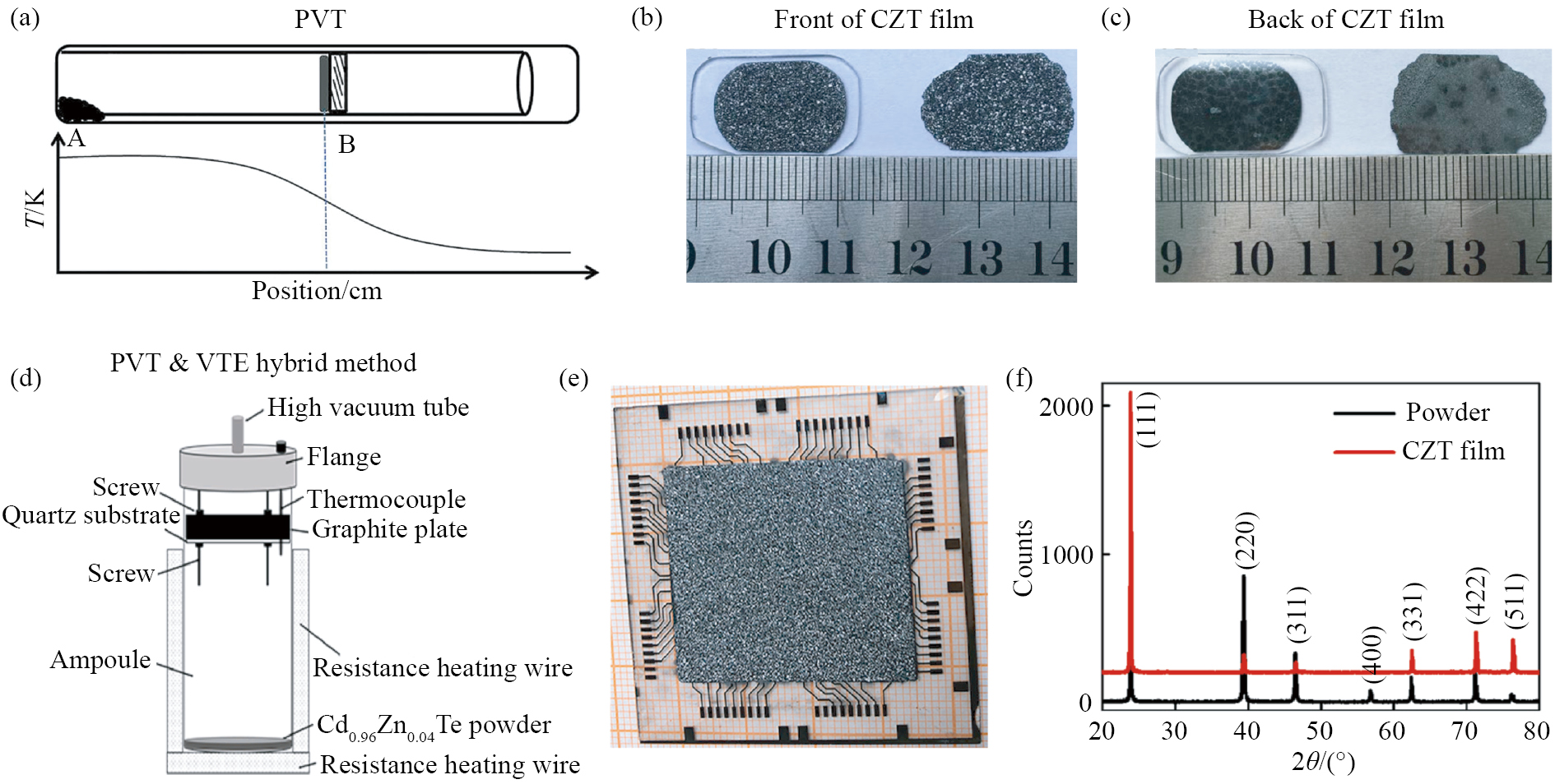
Fig. 2 Preparation of CZT thin film by PVT method and VTE method:(a) Schematic diagram of the preparation of CZT thin film by PVT method[ GAO X Y,SUN H,YANG D Y,et al. Large-area CdZnTe thick film based array X-ray detector[J]. Vacuum,2021,183:109855. 11];(b) Front image of CZT thin film (left side is the film adhered to the substrate,and the right side is the peeled film);(c) Back image of CZT thin film (left side is the film adhered to the substrate,and the right side is the peeled film)[ GAO X Y,SUN H,YANG D Y,et al. Large-area CdZnTe thick film based array X-ray detector[J]. Vacuum,2021,183:109855. 11];(d) Schematic diagram of preparation of CZT thin film by PVT-VTE method[ GAO X Y,SUN H,YANG D Y,et al. Large-area CdZnTe thick film based array X-ray detector[J]. Vacuum,2021,183:109855. 14];(e) CZT thin film depositedon a quartz substrate with Mo array electrodes[ GAO X Y,SUN H,YANG D Y,et al. Large-area CdZnTe thick film based array X-ray detector[J]. Vacuum,2021,183:109855. 14];(f) X-ray diffraction pattern of CZT thin film in (e)[ GAO X Y,SUN H,YANG D Y,et al. Large-area CdZnTe thick film based array X-ray detector[J]. Vacuum,2021,183:109855. 14]
2004年,Mochizuki团队[ TAKAHASHI J,MOCHIZUKI K,HITOMI K,et al. PVT growth of Cd1-xZnxTe (x~0.04) films sensitive to radial rays[J]. Journal of Crystal Growth,2004,269(2-4):448-453. 34]采用PVT法在ITO玻璃上制备了厚度不超过300 μm的Cd0.96Zn0.04Te多晶薄膜,并评估了其应用于辐射探测的潜力。为了提高薄膜的电阻率并降低器件的漏电流,该团队在生长管一端设计了CdCl2粉末的贮存室。薄膜的生长速率与源的温度呈指数关系,而几乎不受CdCl2贮存室温度的影响。CdCl2的引入使薄膜表面没有明显的晶界,但依然粗糙,电阻率提升2个数量级,达到1010 Ω·cm,薄膜虽然对662 keV的γ射线有响应,但并未出现相应的峰。随后,Mochizuki团队[ MOCHIZUKI K,TAKAHASHI J,NAKAMURA N. Thin film growth of Cd1-xZnxTe and its application to X‐ray sensor[J]. Physica Status Solidi C,2015,12(6):528-531. 12]结合热壁法与PVT法在ITO玻璃上制备了不同Zn含量的择优取向为(111)面的CZT多晶薄膜。研究表明,与x=0.04和x=0.50的CZT薄膜相比,x=0.20的CZT薄膜具有最佳的X射线响应特性,证实了该组分CZT薄膜作为X射线传感器的应用潜力。2017年,Gao等[ GAO X Y,ZHU S F,ZHU X H,et al. PVT growth of exfoliated CdZnTe polycrystalline thick films based on stress mismatch mechanism[J]. Journal of Materials Science:Materials in Electronics,2017,28(16):12253-12258. 11]以Cd0.96Zn0.04Te粉末为源,利用PVT法在石英衬底上成功制备了厚度超过600 μm的鳞片状CZT多晶薄膜。由于CZT与衬底热膨胀系数存在较大差异,二者之间的应力失配显著,使得CZT薄膜可从衬底上轻松剥离[图2(a~c)]。基于剥离后的多晶薄膜,Gao等[ GAO X Y,ZHU S F,ZHU X H,et al. PVT growth of exfoliated CdZnTe polycrystalline thick films based on stress mismatch mechanism[J]. Journal of Materials Science:Materials in Electronics,2017,28(16):12253-12258. 11]分别构筑了水平结构和垂直结构两种电极模式的探测器件,测试结果显示,垂直结构的探测器具有更高的暗电阻和更优异的光电特性,这主要是由于载流子在平面内传输时容易受到晶界的散射,导致其收集效率更低。
Zha等[ ZHA G Q,ZHOU H,GAO J N,et al. The growth and the interfacial layer of CdZnTe nano-crystalline films by vacuum evaporation[J]. Vacuum,2011,86(3):242-245. 15]采用VTE法在Si衬底上制备了具有(111)面择优取向的Cd0.9Zn0.1Te纳米晶薄膜,晶粒尺寸约为15 nm。高分辨透射电子显微镜表征结果显示,在薄膜与衬底界面处存在约3 nm的无定型Te层,这一现象归因于Cd与Te之间平衡蒸汽压的差异。研究表明,该无定型界面层的存在是形成纳米晶结构的关键因素。随后,Chander等[ CHANDER S,DHAKA M S. Enhanced structural,electrical and optical properties of evaporated CdZnTe thin films deposited on different substrates[J]. Materials Letters,2017,186:45-48. 13]利用类似的电子束真空蒸发技术,在玻璃、ITO、FTO和硅片等衬底上制备了厚度约为300 nm的CZT多晶薄膜。实验结果表明,不同衬底上沉积的CZT薄膜性能存在显著差异,其中FTO衬底上生长的薄膜结晶性最优、电导率最高,带隙为1.71 eV,在太阳能电池吸收层应用中展现出最佳潜力。Moger等[ MOGER S N,MAHESHA M. Investigation on ZnTe/Cd1-xZnxTe heterostructure for photodetector applications[J]. Sensors and Actuators A:Physical,2020,315:112294. 35]以CdTe和ZnTe为蒸发源,采用VTE法在玻璃衬底上制备了不同组成的ZnTe/CdxZn1-xTe (0.2≤x≤1.0)异质结。其中,ZnTe/Cd0.8Zn0.2Te异质结在可见光照射下具有较高的响应度(0.05~0.24 A/W)和探测率(1010 Jones),揭示了该结构在光电探测器中的应用潜力。
值得注意的是,VTE法不仅适用于平面衬底,也同样适用于表面具有起伏结构的衬底。2021年,Gao等[ GAO X Y,SUN H,YANG D Y,et al. Large-area CdZnTe thick film based array X-ray detector[J]. Vacuum,2021,183:109855. 14]结合PVT和VTE技术,在预先沉积Mo阵列电极(8×8)的石英衬底上制备了面积达5 cm×5 cm、结晶度高的CZT多晶薄膜,该薄膜以(111)为优势取向[图2(d~f)]。基于该薄膜构筑的阵列探测器展现出优异的性能,包括超快的光谱响应、高电阻率(1011 Ω·cm)以及较高的载流子迁移率寿命积(7.2×10⁻³ cm2/V),揭示了CZT薄膜在室温X射线探测与成像领域的应用潜力。
热壁外延法(hot wall epitaxy,HWE)可视为物理气相传输的改进技术,其特点在于通过热壁设计实现更均匀的温度场和气相反应环境。生长腔体壁被独立加热至与源区接近的温度,以消除冷壁效应,减少气相组分在输运过程中的冷凝损失。Cd,Zn,Te蒸汽在热壁环境中充分混合并部分化合(如形成CdTe,ZnTe气相分子),再输运至衬底形成CZT薄膜。HWE法常被用于制备Cd0.96Zn0.04Te薄膜。2003年,Kim等[ KIM B J,WANG J F,LALEV G M,et al. Growth and strain investigation of Cd0.96Zn0.04Te/GaAs by hot-wall epitaxy[J]. Materials Chemistry and Physics,2003,80(3):581-585. 16]采用HWE技术在GaAs衬底上生长了Cd0.96Zn0.04Te薄膜,并系统研究了薄膜厚度对其质量的影响。通过高分辨电子显微镜,直接观察到由晶格常数差异引起的界面位错。应变随外延层厚度的演变规律表明:当CZT薄膜厚度增至5 μm时,外延层中的扩展缺陷密度迅速降低; 当厚度达到20 μm时,应变几乎完全消失,表明增加薄膜厚度有助于获得接近块体单晶质量的外延层。随后,Tang等[ TANG Y H,YIN Y K,CHEN T J. High quality CdZnTe (100)/Si crystal films grown by HWE [C]//Proceedings of ISES World Congress,2007(Vol.I-Vol.V). Berlin,Heidelberg:Springer,2009:1099-1102. 17]在2007年以Cd0.96Zn0.04Te和Zn为双蒸发源,基于自制的HWE法设备,在经过特殊处理后的Si衬底上制备了高质量CZT(100)薄膜。与PVT和VTE方法所得到的表面粗糙的多晶薄膜相比,该薄膜展现出镜面般平整的表面形貌。用扫描电子显微镜进一步证实了薄膜呈现单一取向的柱状生长模式,标志着热壁外延技术在CZT薄膜制备领域取得重要突破。然而,此后十余年内,关于HWE法制备CZT薄膜的研究相对较少。直到2021年,Vuichyk等[ VUICHYK M,RASHKOVETS'KYI L,LAVORYK S,et al. Forming of CdZnTe thin films grown by hot wall epitaxy and their properties[J]. Physics and Chemistry of Solid State,2021,22(4):638-643. 18]才报道了基于HWE法在较低衬底温度(约100 ℃)制备的30~810 nm厚CZT薄膜,但所得薄膜由众多百纳米级晶粒拼接而成,表面仍较为粗糙,表明在低温条件下制备高质量薄膜仍具挑战性。
Fig. 3 Preparation of CZT thin films by magnetron sputtering:(a) Schematic diagram of magnetron sputtering;Morphology of CZT thin films prepared at substrate temperatures of (b) 200 ℃,(c)300 ℃ and (d) 400 ℃[ MALKAS H,KAYA S,YILMAZ E. Effects of substrate temperature on the microstructure and morphology of CdZnTe thin films[J]. Journal of Electronic Materials,2014,43(11):4011-4017. 19];(e) Multilayer CZT thin films prepared bymagnetron sputtering[ MALKAS H,KAYA S,YILMAZ E. Effects of substrate temperature on the microstructure and morphology of CdZnTe thin films[J]. Journal of Electronic Materials,2014,43(11):4011-4017. 20];(f) Surface roughness statistics of CZT thin films with different numbers of layers[ MALKAS H,KAYA S,YILMAZ E. Effects of substrate temperature on the microstructure and morphology of CdZnTe thin films[J]. Journal of Electronic Materials,2014,43(11):4011-4017. 20]
Malkas等[ MALKAS H,KAYA S,YILMAZ E. Effects of substrate temperature on the microstructure and morphology of CdZnTe thin films[J]. Journal of Electronic Materials,2014,43(11):4011-4017. 19]以直径10.16 cm(4英寸)Cd0.9Zn0.1Te为靶材,利用磁控溅射法在玻璃衬底上制备了厚度为200 nm的CZT薄膜。研究表明,衬底温度对薄膜的结构和形貌具有显著影响。通过比较200,300和400 ℃三种不同衬底温度下制备的薄膜形貌发现,随着衬底温度的升高,原子在衬底表面的迁移和扩散速率增加,薄膜中的晶粒尺寸逐渐增大,且薄膜表面平整度显著提升[图3(b~d)]。Gao等[ GAO X Y,ZHU X H,SUN H,et al. Preparation and characterization of CdZnTe multilayer films by repeated RF magnetron sputtering[J]. Journal of Materials Science:Materials in Electronics,2017,28(5):4467-4474. 20]采用磁控溅射法在ITO衬底上制备了多层CZT薄膜,随着重复沉积次数的增加,薄膜厚度从1360 nm增至9230 nm[图3(e)]。此外,重复沉积可有效消除薄膜与衬底之间的热应力失配,从而提高薄膜的附着力和结晶质量,增大晶粒尺寸[图3(f)]。Zeng等[ ZENG D,MU Y,MENG J,et al. Properties of Al doped CdZnTe film by aluminium induced crystallization[J]. Surface Engineering,2016,32(3):190-193. 36]以高纯Al和Cd0.9Zn0.1Te为靶,采用磁控溅射法制备了Al掺杂的CZT薄膜。掺Al的CZT薄膜在化学组成上更接近靶材的原始配比,电阻率显著提高至8.5×10⁹ Ω·cm,较未掺杂的CZT薄膜电阻率(5.6×10⁷ Ω·cm)提升了近2个数量级,这可能是因为Al原子作为施主杂质可有效补偿薄膜中的Cd空位缺陷。
Fig. 4 CZT thin film prepared by CSS method:(a) Schematic diagram of the CSS system[ COLEGROVE E,ALBIN D S,MOUTINHO H R,et al. Scalable ultrafast epitaxy of large-grain and single-crystal Ⅱ-Ⅳ semiconductors[J]. Scientific Reports,2020,10(1):2426. 37];(b) Schematic illustration of the CZT thin film preparation process by CSS;(c) Morphology of polycrystalline CZT thin films[ 苏虹,査钢强,高俊宁,等. 近空间升华法制备CdZnTe厚膜及其性能研究[J]. 功能材料,2012,43(23):3322-3324,3328. 38] and (d) CZT micro pillar film prepared by CSS[ HUANG J,CHEN Z R,BIE J Y,et al. Novel CdZnTe micro pillar films deposited by CSS method[J]. Materials Letters,2020,263:127277. 39];(e) XRD pattern of polycrystalline CZT thin film prepared by CSS[ 苏虹,査钢强,高俊宁,等. 近空间升华法制备CdZnTe厚膜及其性能研究[J]. 功能材料,2012,43(23):3322-3324,3328. 38];(f) CZT thin film deposited on a thin-film transistor[ LI Y W,ZHANG W Y,CAO K,et al. Cracking mechanism of CdZnTe polycrystalline film deposited on TFT circuit board at high temperature by close-spaced sublimation method[J]. Materials Science in Semiconductor Processing,2021,131:105821. 40];(g) Morphology of single-crystal CZT thin film prepared by CSS[ LI Y W,ZHANG W Y,CAO K,et al. Cracking mechanism of CdZnTe polycrystalline film deposited on TFT circuit board at high temperature by close-spaced sublimation method[J]. Materials Science in Semiconductor Processing,2021,131:105821. 23];(h) XRD pattern of single-crystal CZT thinfilm prepared by CSS[ LI Y W,ZHANG W Y,CAO K,et al. Cracking mechanism of CdZnTe polycrystalline film deposited on TFT circuit board at high temperature by close-spaced sublimation method[J]. Materials Science in Semiconductor Processing,2021,131:105821. 23];(i) CZT thin film of 5.08 cm (2 inch) prepared by CSS[ LI Y W,ZHANG W Y,CAO K,et al. Cracking mechanism of CdZnTe polycrystalline film deposited on TFT circuit board at high temperature by close-spaced sublimation method[J]. Materials Science in Semiconductor Processing,2021,131:105821. 24]
衬底材料会显著影响CZT薄膜的生长行为。不同衬底上,CSS法制备的CZT薄膜可分为多晶和单晶两种形态。研究表明,在Si,FTO玻璃等衬底上沉积的CZT薄膜通常呈现多晶结构,并表现出(111)晶面择优取向生长特性[图4(c~f)][ 苏虹,査钢强,高俊宁,等. 近空间升华法制备CdZnTe厚膜及其性能研究[J]. 功能材料,2012,43(23):3322-3324,3328. 38, YU B,XU C G,XIE M X,et al. Deposition of CdZnTe films with CSS method on different substrates for nuclear radiation detector applications[J]. Crystals,2022,12(2):187. ZHANG Y L,WANG L J,XU R,et al. The microstructure,optical and electrical property of CdZnTe thick films grown from a CSS method[J]. Journal of Crystal Growth,2015,431:10-14. HUANG J,GU Q M,YANG F,et al. Growth and properties of CdZnTe films on different substrates[J]. Surface and Coatings Technology,2019,364:444-448. WU Y L,XU H T,JI H H,et al. Growth of Cd1-xZnxTe thin films with high Zn content by close-spaced sublimation[J]. Vacuum,2016,132:106-110. WANG Q F,HUANG H F,XU K,et al. Enhancement of detection performances of cadmium zinc telluride (CdZnTe) radiation detectors through sapphire substrates[J]. Journal of Alloys and Compounds,2025,1010:177952. TAO J,XU H T,ZHANG Y L,et al. Interface chemistry of CdZnTe films studied by a peel-off approach[J]. Applied Surface Science,2016,388:180-184. 41-46]。苏虹等[ 苏虹,査钢强,高俊宁,等. 近空间升华法制备CdZnTe厚膜及其性能研究[J]. 功能材料,2012,43(23):3322-3324,3328. 38]于2012年采用CSS法在FTO玻璃上制备了厚度为40~90 μm的CZT多晶薄膜,该薄膜虽然均匀致密,但由多取向晶粒拼接而成,表面较为粗糙[图4(c)],且薄膜中晶粒的尺寸随着生长时间的延长而逐渐增大。2019年,Huang等[ HUANG J,GU Q M,YANG F,et al. Growth and properties of CdZnTe films on different substrates[J]. Surface and Coatings Technology,2019,364:444-448. 43]研究发现,相较于Si和FTO玻璃衬底,在抛光的CZT衬底上生长的薄膜具有更大的晶粒尺寸、更优的结晶质量以及更好的结构完整性。此外,该衬底上薄膜的生长速率可达3.45 μm/min,且Zn含量更高,表现出更低的漏电流特性,更适合用于高能粒子探测。随后该团队发现,在石英衬底上引入单层石墨烯后,CZT薄膜由平面生长模式转变为垂直柱状生长,形成直径约5 μm、长度达57 μm的微柱结构[图4(d)][ HUANG J,CHEN Z R,BIE J Y,et al. Novel CdZnTe micro pillar films deposited by CSS method[J]. Materials Letters,2020,263:127277. 39]。基于该结构薄膜制备的Au/BGZO/CZT/石墨烯/石英器件表现出优异的可见光响应特性,展现了其在光电子器件中的应用潜力。Wang等[ WANG Q F,HUANG H F,XU K,et al. Enhancement of detection performances of cadmium zinc telluride (CdZnTe) radiation detectors through sapphire substrates[J]. Journal of Alloys and Compounds,2025,1010:177952. 45]在2025年的最新研究探索了在成本更低的蓝宝石衬底上制备CZT薄膜。研究发现,薄膜最佳生长条件为蒸发源675 ℃,衬底450 ℃,优化后薄膜载流子迁移率寿命积可达6.3×10⁻⁴ cm2/V,接近单晶薄膜。基于蓝宝石衬底制备的CZT薄膜构建的探测器在检测59.54 keV γ射线时展现出接近18.9%的能量分辨率,较其他报道有显著提升[ WAN X,CAO K,LI Y,et al. Preparation and characterization of large-sized CdZnTe epitaxial single crystal[J]. Nuclear Instruments and Methods in Physics Research Section A:Accelerators,Spectrometers,Detectors and Associated Equipment,2023,1056:168625. 24]。
需要特别指出的是,采用CSS技术可直接在薄膜晶体管(TFT)基板上制备CZT多晶薄膜[图4(f)][ LI Y W,ZHANG W Y,CAO K,et al. Cracking mechanism of CdZnTe polycrystalline film deposited on TFT circuit board at high temperature by close-spaced sublimation method[J]. Materials Science in Semiconductor Processing,2021,131:105821. 40],这一突破性进展为CZT薄膜在光电探测器等领域的直接应用提供了重要技术路径。目前,沉积过程中衬底温度过高会导致TFT电路板上的CZT薄膜发生破裂:高温会释放Al膜与ITO膜之间的界面应力并诱发形成微小凸起,致使ITO/CZT界面的结合强度超过ITO/Mo/Al/Mo界面,最终引发CZT薄膜的剥离失效。通过优化CSS设备的温控系统,将沉积温度稳定控制在150~300 ℃范围内,有望实现TFT基板上CZT薄膜的低温可靠生长。
当生长衬底与外延材料晶格匹配时,外延层可能呈现单一取向。CdTe的晶格常数为6.481 Å,ZnTe的晶格常数为6.103 Å,依据Vegard定律可计算出,当CdTe与ZnTe的摩尔比为9∶1时,Cd0.9Zn0.1Te的晶格常数为6.443 Å。GaAs,GaSb衬底均具有与CZT相同的闪锌矿结构,且已被证实可用于外延生长CZT单晶薄膜[ WU S H,ZHA G Q,CAO K,et al. The growth of CdZnTe epitaxial thick film by close spaced sublimation for radiation detector[J]. Vacuum,2019,168:108852. WAN X,CAO K,LI Y,et al. Preparation and characterization of large-sized CdZnTe epitaxial single crystal[J]. Nuclear Instruments and Methods in Physics Research Section A:Accelerators,Spectrometers,Detectors and Associated Equipment,2023,1056:168625. LI Y,CAO K,ZHA G Q,et al. An alternative GaSb substrate allowing close-spaced sublimation of Cd0.9Zn0.1Te epitaxial thick film for radiation detectors[J]. Materials Science in Semiconductor Processing,2022,147:106688. 23-25, LIU Y,WU W,ZHANG X L,et al. Investigation of the CdZnTe (211) and (133) films grown on GaAs (211) controlled by temperature:experiment and first-principles calculations[J]. Applied Surface Science,2024,649:159154. GAO J N,JIE W Q,YUAN Y Y,et al. One-step fast deposition of thick epitaxial CdZnTe film on (001)GaAs by close-spaced sublimation[J]. CrystEngComm,2012,14(5):1790-1794. LIU Y,ZHA G Q,CAO K,et al. Growth of CdZnTe (211) epilayers on GaAs by close spaced sublimation as an alternative substrate for HgCdTe growth[J]. Infrared Physics & Technology,2023,133:104857. 47-49]。其中,GaAs(001)衬底的晶格常数为5.653 Å,Cd0.1Zn0.9Te薄膜在其上外延晶格失配为13.9%。2012年,Gao等[ GAO J N,JIE W Q,YUAN Y Y,et al. One-step fast deposition of thick epitaxial CdZnTe film on (001)GaAs by close-spaced sublimation[J]. CrystEngComm,2012,14(5):1790-1794. 48]利用CSS法在GaAs(001)衬底上生长了CZT(001)单晶薄膜。研究结果表明:生长初期,薄膜由不同取向的小晶粒组成,呈多晶态; 随着时间的延长,晶粒可通过自组装与横向拼接实现多晶薄膜向单晶薄膜的转变。2019年,Wu等[ WU S H,ZHA G Q,CAO K,et al. The growth of CdZnTe epitaxial thick film by close spaced sublimation for radiation detector[J]. Vacuum,2019,168:108852. 23]采用CSS在GaAs(001)衬底上制备出厚度达1.1 mm、幅面尺寸为12 mm×12 mm的CZT单晶薄膜[图4(g,h)]。该薄膜X射线摇摆曲线半峰宽约166″,位错密度为1.05×105 cm−2,载流子迁移率寿命积为1.0×10⁻³ cm2/V,电子迁移率达到750 cm2/(V·s)。2023年,Wan等[ WAN X,CAO K,LI Y,et al. Preparation and characterization of large-sized CdZnTe epitaxial single crystal[J]. Nuclear Instruments and Methods in Physics Research Section A:Accelerators,Spectrometers,Detectors and Associated Equipment,2023,1056:168625. 24]在GaAs(001)衬底上外延生长了厚度超过1 mm、尺寸达5.08 cm(2英寸)的CZT单晶薄膜[图4(i)],进一步提升了薄膜的制备规模。然而,薄膜并不完全均匀,中心区域薄膜质量优于边缘区域,表现为更低的位错密度、更高的电阻率、更大的载流子迁移率寿命积以及更高的X射线探测灵敏度。这表明,大尺寸CZT单晶薄膜在均匀性方面仍有待进一步提升。
GaSb(001)衬底的晶格常数为6.096 Å,Cd0.1Zn0.9Te薄膜在其上外延晶格失配率仅为5.7%,低于GaAs(001)衬底,理论上GaSb衬底上的薄膜具有更高的质量。Li等[ LI Y,CAO K,ZHA G Q,et al. An alternative GaSb substrate allowing close-spaced sublimation of Cd0.9Zn0.1Te epitaxial thick film for radiation detectors[J]. Materials Science in Semiconductor Processing,2022,147:106688. 25]采用CSS法在GaSb(001)衬底上成功外延生长了厚度约88 μm的CZT单晶薄膜。该薄膜表面平整,X射线摇摆曲线半峰宽约173″,电阻率达9.09×10⁹ Ω·cm,载流子迁移率寿命积为3.55×10⁻⁴ cm2/V。基于该薄膜构筑的探测器对241Am@59.54 keV γ射线能谱分辨率达到17%,展现了CZT薄膜在低成本X射线探测与成像中的应用潜力。为进一步提升薄膜质量,李阳等[ 李阳,曹昆,介万奇,等. 热处理GaSb衬底对近距离升华法制备CdZnTe外延膜的影响[J]. 人工晶体学报,2024,53(10):1705-1711. 50]研究了热处理GaSb衬底对外延CZT薄膜质量的影响。结果表明,将GaSb衬底经600 ℃处理180 s后,可去除衬底表面大部分氧化物并保持衬底相对平整,该衬底上外延的CZT薄膜质量显著提升,X射线摇摆曲线半峰宽约94″,接近已报道的块状CZT单晶的结晶质量[ MACKENZIE J,KUMAR F J,CHEN H. Advancements in THM-grown CdZnTe for use as substrates for HgCdTe[J]. Journal of Electronic Materials,2013,42(11):3129-3132. 51]。
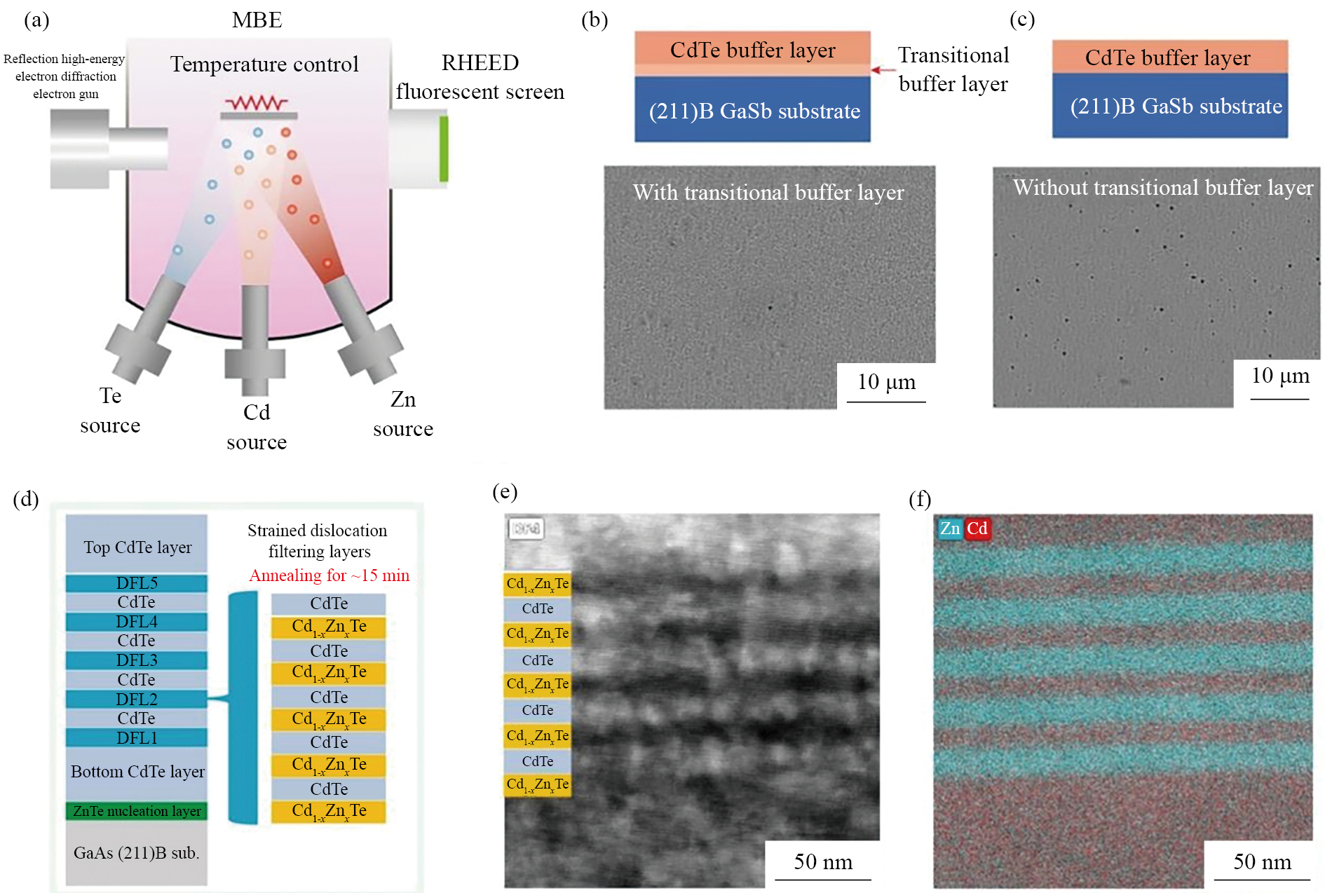
Fig. 5 CZT thin films and CZT/CdTe superlattice prepared by MBE method:(a) Schematic diagram of MBE system structure;(b,c) Surface morphology of CdTe thin films prepared by MBE,where (b) uses alternately stacked ZnTe/CdTe as a transition layer[ LEI W,REN Y L,MADNI I,et al. Low dislocation density MBE process for CdTe-on-GaSb as an alternative substrate for HgCdTe growth[J]. Infrared Physics & Technology,2018,92:96-102. 27];(d) Schematic diagram of ZnTe(133) thin film grown on a GaAs(211)B substrate,employing a CZT/CdTe superlattice as adislocation filtering layer[ PAN W W,GU R J,ZHANG Z K,et al. Defect engineering in MBE-grown CdTe buffer layers on GaAs (211)B substrates[J]. Journal of Electronic Materials,2022,51(9):4869-4883. 28];(e) Cross-sectional TEM image and (f) cross-sectional EDS elementalmapping image of CZT/CdTe superlattice in (d)[ PAN W W,MA S,SUN X,et al. Structural properties of MBE-grown CdTe (133)B buffer layers on GaAs (211)B substrates with CdZnTe/CdTe superlattice-based dislocation filtering layers[J]. Journal of Applied Physics,2023,133(18):185301. 29]
2000年,Kozlovsky等[ KOZLOVSKY V I,KRYSA A B,KOROSTELIN Y V,et al. MBE growth and characterization of ZnTe epilayers and ZnCdTe/ZnTe structures on GaAs(100) and ZnTe(100) substrates[J]. Journal of Crystal Growth,2000,214-215:35-39. 26]以高纯Te,Zn,Cd为源,在ZnTe衬底上生长了Cd0.1Zn0.9Te薄膜,形成了高质量的量子阱结构。2018年,Lei等[ LEI W,REN Y L,MADNI I,et al. Low dislocation density MBE process for CdTe-on-GaSb as an alternative substrate for HgCdTe growth[J]. Infrared Physics & Technology,2018,92:96-102. 27]利用MBE在GaSb(211)B衬底上成功制备了CdTe薄膜[图5(b,c)]。研究表明,在衬底上预先引入150~200 nm厚的缓冲层后,外延生长的CdTe薄膜位错密度从106 cm−2降低至105 cm−2。该缓冲层由交替排列的ZnTe/CdTe组成,不仅有效减少了CdTe薄膜中的失配位错,同时作为缺陷和杂质的吸收层,显著提升了外延薄膜的晶体质量。此外,近年来,研究者们尝试采用MBE技术在GaAs(211)B衬底上外延生长CdTe(133)B薄膜作为缓冲层,用于HgCdTe薄膜的外延生长[ PAN W W,GU R J,ZHANG Z K,et al. Defect engineering in MBE-grown CdTe buffer layers on GaAs (211)B substrates[J]. Journal of Electronic Materials,2022,51(9):4869-4883. PAN W W,MA S,SUN X,et al. Structural properties of MBE-grown CdTe (133)B buffer layers on GaAs (211)B substrates with CdZnTe/CdTe superlattice-based dislocation filtering layers[J]. Journal of Applied Physics,2023,133(18):185301. 28-29]。为进一步优化CdTe缓冲层质量,研究者们在缓冲层与衬底之间引入了CZT/CdTe超晶格作为位错过滤层[图5(d~f)]。实验结果表明,该位错过滤层能显著降低CdTe缓冲层的表面粗糙度,并将位错腐蚀坑密度降至105 cm−2量级。
金属有机化学气相沉积法(metal-organic chemical vapor deposition,MOCVD)是一种可控性强的薄膜沉积方法。MOCVD法通常以金属有机前驱体和氢化物气体为反应源,两种前驱体在相对较低的温度下发生化学反应,进而在衬底表面沉积目标材料薄膜。Cohen等[ COHEN K,STOLYAROVA S,AMIR N,et al. MOCVD growth of ordered Cd1-xZnxTe epilayers[J]. Journal of Crystal Growth,1999,198-199:1174-1178. 31]以二乙基锌、二甲基镉和二乙基碲作为金属有机前驱体,以氢气为载气,在CdTe(100)衬底上沉积了有序的CZT外延层[图6(a)]。CZT薄膜中Zn组分的含量由生长温度与反应腔中的气体组分共同决定,成分控制过程简单。类似地,Devyatykh等[ DEVYATYKH G G,MOISEEV A N,KOTKOV A P,et al. Metalorganic vapor-phase epitaxy of ZnTe and CdZnTe on GaAs[J]. Inorganic Materials,2002,38(2):99-105. 32]采用MOCVD方法分别在GaAs(111)B和GaAs(100)衬底上外延生长了CdTe/ZnTe异质结和CZT薄膜[图6(b~d)],所得薄膜表面平整。X射线衍射摇摆曲线测试结果显示,CZT薄膜的半峰宽为5′~8′,表明其结晶质量较高。研究发现,沉积温度对薄膜的生长速率、成分以及结构完整性均有显著影响,通常温度越高,薄膜中的Zn含量越高。然而,影响薄膜结构质量的关键因素仍是衬底取向:在GaAs(100)衬底上外延的Cd1-xZnxTe(100)薄膜,其结构完整性优于在GaAs(111)B衬底上生长的Cd1-xZnxTe(111)薄膜。
Fig. 6 Preparation of CdTe/ZnTe heterostructure and CZT thin films by MOCVD:(a) Schematic illustration of MOCVD process for CZT thin film deposition;(b) Variation curve of ZnTe molar ratio in CZT thin films as a function of growth temperature[ DEVYATYKH G G,MOISEEV A N,KOTKOV A P,et al. Metalorganic vapor-phase epitaxy of ZnTe and CdZnTe on GaAs[J]. Inorganic Materials,2002,38(2):99-105. 32];(c) Surface morphology of CdTe/ZnTe heterostructure prepared by MOCVD[ DEVYATYKH G G,MOISEEV A N,KOTKOV A P,et al. Metalorganic vapor-phase epitaxy of ZnTe and CdZnTe on GaAs[J]. Inorganic Materials,2002,38(2):99-105. 32];(d) Surface morphology of CZT thin film prepared by MOCVD[ DEVYATYKH G G,MOISEEV A N,KOTKOV A P,et al. Metalorganic vapor-phase epitaxy of ZnTe and CdZnTe on GaAs[J]. Inorganic Materials,2002,38(2):99-105. 32]
MOCVD的优势在于兼顾了生长速率和薄膜质量,通过调控有机前驱体的流量比,可在较高速率下生长出高质量单晶薄膜,同时具备优异的大面积均匀性和批次重复性,适合10.16~15.24 cm (4~6英寸)衬底的大规模生产。然而,MOCVD也面临工艺复杂且成本高的挑战:高纯度有机金属源价格昂贵且具有毒性,增加了安全和环保压力; 反应温度和气相动力学对薄膜质量影响极大,需精确优化数十项参数。尽管基于平衡薄膜性能与制备成本MOCVD被视为优选方案,但目前以该方法制备的CZT薄膜在尺寸和质量方面尚未展现出优势。
CZT薄膜生长参数是决定薄膜质量的关键因素,其中温度是核心工艺参数之一,对薄膜的沉积动力学过程和微观结构具有决定性影响。具体而言,温度不仅能直接调控薄膜的沉积速率,还会显著影响薄膜的晶粒尺寸、结晶质量等。通过精确控制生长温度,可实现对薄膜微观结构和性能的有效调控。Huang等[ HUANG J,WANG L J,TANG K,et al. Growth of high quality CdZnTe films by close-spaced sublimation method[J]. Physics Procedia,2012,32:161-164. 52]系统研究了沉积参数对CSS法制备CZT薄膜生长速率的影响。结果表明:衬底温度在450 ℃以下时,生长速率保持恒定,仅取决于蒸发源温度; 当衬底温度高于450 ℃时,生长速率下降; 当生长源温度为650 ℃时,薄膜沉积速率最大可超过5 μm/min。Jiang等[ JIANG R,KANG Y,CAO K,et al. Optimized substrate temperature for high-quality CdZnTe epitaxial film in X-ray flat panel detectors[J]. Vacuum,2024,230:113705. 53]进一步探究了在不同衬底温度下沉积的CZT薄膜质量变化。研究结果表明,随着衬底温度的升高,CZT薄膜表面出现逆升华现象并形成凹坑,凹坑尺寸和深度随温度的升高而增大。这一现象可归因于Zn-Te键与Cd-Te键的键能差异:在高温条件下,键能较低的Cd-Te键优先断裂,导致Zn元素在薄膜表面富集,形成富Zn表层; Zn含量的增加使薄膜带隙增大,进而导致漏电流降低,电阻率增大,其中在500 ℃下制备的CZT薄膜电阻率高达1011 Ω·cm。基于优化衬底温度下制备的CZT薄膜构筑的探测器,展现出优异的光电性能,其响应时间在上升阶段和下降阶段分别为2 ms和4 ms。值得注意的是,该探测器在X射线照射下可清楚地区分空气、塑料和金属,展现出在下一代高灵敏度X射线探测系统中的巨大应用潜力。
由于GaAs衬底与CZT薄膜之间存在较大的晶格失配,外延过程中呈现典型的岛状生长模式(Volmer-Weber),失配晶畴在拼接融合时易产生穿透位错,最终在薄膜表面形成生长坑[ CAO K,JIE W Q,ZHA G Q,et al. Nucleation and islands growth of CdZnTe(001) epitaxial films on GaAs(001) substrates by close spaced sublimation[J]. Journal of Crystal Growth,2018,498:197-201. CAO K,JIE W Q,ZHA G Q,et al. Origin and evolution of threading dislocation in CdZnTe(001)/GaAs(001) epilayer grown by close spaced sublimation[J]. Applied Surface Science,2020,504:144431. CAO K,JIE W Q,ZHA G Q,et al. Analysis of dislocations in CdZnTe epitaxial film with kelvin probe and conductive atomic force microscopy[J]. Journal of Electronic Materials,2020,49(6):3907-3912. CHENG R Y,ZHA G Q,CAO K,et al. The growth pits filling mechanism of CdZnTe epitaxial film prepared by close-spaced sublimation based on the first-principles calculation[J]. Journal of Crystal Growth,2023,618:127303. 54-57]。当衬底温度较低时,孪晶与薄膜表面的交界处还可能产生针状缺陷[ CHENG R Y,CAO K,ZHA G Q,et al. Formation mechanism and elimination of needle defects on CdZnTe epitaxial films prepared by close-spaced sublimation[J]. Applied Surface Science,2024,657:159813. 58]。通过提高生长温度、降低初始成核速率以及改善成核层质量,有望有效降低针状缺陷的密度。
Guo等[ GUO Q X,NADA M,DING Y L,et al. Low-temperature buffer layer effects on the quality of ZnTe epilayers grown on sapphire substrates[J]. Journal of Applied Physics,2010,107(12):123525. 59]在蓝宝石衬底上外延生长ZnTe薄膜时,采用了低温成核(320 ℃)-高温生长(440 ℃)的两步生长法,结果表明该方法可以显著提高ZnTe薄膜的表面平整性、结晶质量及光学性质,且低温层的厚度是影响ZnTe薄膜质量的关键因素。当低温层厚度为21 nm时,外延生长的ZnTe薄膜质量最高。产生这一结果的原因,可能是低温层可减小并释放蓝宝石衬底和ZnTe薄膜之间由于晶格常数差异产生的应力,从而在低温层上生长出高质量的ZnTe薄膜。受此启发,Cao等[ CAO K,JIE W Q,ZHA G Q,et al. Improvement of crystalline quality of CdZnTe epilayers on GaAs(001) substrates with a two-step growth by close spaced sublimation[J]. Vacuum,2019,164:319-324. 60]开发了一种基于CSS的两步法工艺,在GaAs(001)衬底上成功实现了高质量CZT薄膜的外延生长。第一步的低温预生长阶段(350 ℃)可形成更为致密的成核层,这有效促进了后续晶粒融合和缺陷的湮灭过程。通过X射线摇摆曲线分析和光致发光光谱表征,证实了采用第一步350 ℃低温生长与第二步430 ℃高温生长相结合的策略,可获得具有最优晶体质量的CZT薄膜。值得注意的是,当第二步生长温度从430 ℃提升至530 ℃和600 ℃时,受热应力增大和Zn含量增加的双重影响,薄膜的晶体质量呈现下降趋势。进一步的电流-电压特性测试和α粒子响应实验结果表明,CZT薄膜的电学性能与其结晶质量呈现正相关关系:结晶质量越优异,薄膜的电阻率越高,同时载流子输运性能也越突出。
高温成核-低温生长法多用于快速生长高质量CZT薄膜。Li等[ LI Y,CAO K,ZHA G Q,et al. An alternative GaSb substrate allowing close-spaced sublimation of Cd0.9Zn0.1Te epitaxial thick film for radiation detectors[J]. Materials Science in Semiconductor Processing,2022,147:106688. 25]采用该两步法策略,分别在GaAs和GaSb衬底上实现了CZT单晶薄膜的外延生长。在GaAs衬底上生长时,第一步衬底温度设定为560 ℃,该温度有助于在界面处形成高质量的成核层,因为较高的衬底温度能够促进晶粒的取向一致,增大畴区尺寸,减少畴界面和位错。然而,过高的温度可能导致薄膜发生逆升华。第二步中,衬底温度降低至450 ℃,此时蒸发源与衬底之间的温差增大,从而可提高薄膜生长速率,实现CZT单晶薄膜的快速生长。对于GaSb衬底,由于其熔点较低(710 ℃),因此两步法通过调控生长源的温度实现高质量薄膜制备。第一步,将源温度保持在600 ℃,以便在较低的源温度下形成致密的薄膜; 第二步,将源温度升高至710 ℃,以更快的速度形成较厚的薄膜。在此过程中,GaSb的衬底温度始终保持在180 ℃。这种高温成核-低温生长的两步法工艺,可在较短时间内制备出厚度达数百微米的高质量CZT薄膜。
Fig. 7 (a) Schematic diagram of the growth process of CZT thin film with a buffer layer;(b) Cross-sectional SEM image of the CdZnTe/ZnTe/GaAs thin film[ LIU Y,ZHANG X L,GAO Z H,et al. Growth of high quality CdZnTe (133) epilayers on GaAs (211) substrate with Zn1-xCdxTe/ZnTe buffer layer by close spaced sublimation[J]. Journal of Alloys and Compounds,2024,977:173261. 62];Surface morphology of CZT thin film grown on (c) GaAs and (d) ZnTe/GaAs substrates after etching[ LIU Y,ZHANG X L,GAO Z H,et al. Growth of high quality CdZnTe (133) epilayers on GaAs (211) substrate with Zn1-xCdxTe/ZnTe buffer layer by close spaced sublimation[J]. Journal of Alloys and Compounds,2024,977:173261. 62];(e) Cross-sectional TEM image and EDS elemental mapping of CdZnTe/ZnTe/GaSb thin film[ LI Y,ZHANG X L,WAN X,et al. Improvement of crystallinity of CdZnTe epilayers on GaSb substrates by ZnTe buffer layer[J]. Vacuum,2023,217:112551. 63];(f) Cross-sectionalEBSD image of CZT thin film grown on GaSb and (g) ZnTe/GaSb substrate[ LI Y,ZHANG X L,WAN X,et al. Improvement of crystallinity of CdZnTe epilayers on GaSb substrates by ZnTe buffer layer[J]. Vacuum,2023,217:112551. 63]
Leo等[ LEO G,LONGO M,LOVERGINE N,et al. Influence of a ZnTe buffer layer on the structural quality of CdTe epilayers grown on (100)GaAs by metalorganic vapor phase epitaxy[J]. Journal of Vacuum Science & Technology B:Microelectronics and Nanometer Structures Processing,Measurement,and Phenomena,1996,14(3):1739-1744. 61]研究了在GaAs(100)衬底上外延CdTe薄膜时,不同厚度ZnTe缓冲层对外延层的影响。研究发现:当ZnTe缓冲层厚度在0~10 nm范围内时,随着外延界面失配位错的减少以及ZnTe中缺陷密度的快速降低,CdTe薄膜的结晶质量显著提升; 当ZnTe缓冲层厚度增加至300~500 nm时,CdTe薄膜的结晶质量达到最佳。这种缓冲层厚度对薄膜形貌和质量的影响,可能与ZnTe缓冲层的缺陷分布和表面粗糙度有关。具体而言:当ZnTe缓冲层厚度为300 nm时,CdTe薄膜的表面粗糙度最低; 而当ZnTe缓冲层厚度超过500 nm时,CdTe薄膜的粗糙度迅速增大。类似地,Liu等[ LIU Y,ZHANG X L,GAO Z H,et al. Growth of high quality CdZnTe (133) epilayers on GaAs (211) substrate with Zn1-xCdxTe/ZnTe buffer layer by close spaced sublimation[J]. Journal of Alloys and Compounds,2024,977:173261. 62]通过在GaAs(211)衬底上引入ZnTe缓冲层,成功制备了高质量的Cd0.96Zn0.04Te(133)薄膜[图7(b)],该方法有望应用于外延HgCdTe。ZnTe缓冲层的引入,显著提升了CZT薄膜的晶体质量,使腐蚀坑密度从3.2×105 cm−2降低至2.6×105 cm−2[图7(c,d)],X射线摇摆曲线半峰宽从57″减小到34″,表面粗糙度从9.88 nm降至3.69 nm。此外,ZnTe缓冲层的引入促进了CZT薄膜与ZnTe界面处CuPt型有序CZT区的形成,从而有效地释放了GaAs与ZnTe界面处的失配应变。
在GaSb衬底上引入ZnTe缓冲层,同样有助于提高外延CZT薄膜的结晶质量[图7(e~g)]。Li等[ LI Y,ZHANG X L,WAN X,et al. Improvement of crystallinity of CdZnTe epilayers on GaSb substrates by ZnTe buffer layer[J]. Vacuum,2023,217:112551. 63]的研究表明,在GaSb衬底上直接沉积CZT薄膜,可能导致高密度的晶格失配孪晶和亚晶畴区的形成[图7(f)]。然而,若在GaSb衬底上先沉积约3 μm的ZnTe缓冲层,再以其作为外延生长CZT薄膜的衬底,则可有效抑制外延层中晶格失配孪晶和亚晶畴区的产生[图7(g)]。当沉积温度为495 K时,可获得表面光滑且结晶质量优异的ZnTe缓冲层,进而制备出高质量的CZT外延层。此时,CZT薄膜的(004)峰X射线摇摆曲线半峰宽仅为85″。
Fig. 8 (a) Schematic diagram of CZT thin films annealed in different atmospheres;(b) XRD patterns and (c) electrical test results of CZT thin films annealed at different temperatures in air atmosphere[ CHANDER S,DHAKA M S. Optimization of structural,optical and electrical properties of CdZnTe thin films with the application of thermal treatment[J]. Materials Letters,2016,182:98-101. 64];(d) Transmission spectra before and after annealing in CdCl2 atmosphere[ HUANG J,WANG L J,TANG K,et al. Growth of high quality CdZnTe films by close-spaced sublimation method[J]. Physics Procedia,2012,32:161-164. 52];(e,f) Changes in dislocation etch pit density on surface of CZT thin films before and after annealing in Te2 atmosphere[ WAN X,LI Y,TAN T T,et al. Effects of annealing in Te2 atmosphere on photoelectric properties and carrier transport properties of CdZnTe films[J]. Materials Science in Semiconductor Processing,2023,153:107158. 65];(g) Changes in resistivity of CZT thin films before and after different annealing durations in Te2 atmosphere[ WAN X,LI Y,TAN T T,et al. Effects of annealing in Te2 atmosphere on photoelectric properties and carrier transport properties of CdZnTe films[J]. Materials Science in Semiconductor Processing,2023,153:107158. 65]
Chander等[ CHANDER S,DHAKA M S. Optimization of structural,optical and electrical properties of CdZnTe thin films with the application of thermal treatment[J]. Materials Letters,2016,182:98-101. 64]采用电子束真空镀膜技术,在玻璃和ITO衬底上沉积了厚度为400 nm的CZT薄膜,并系统研究了150,300和400 ℃三个退火温度对CZT薄膜结构与性质的影响。研究结果表明,随着退火温度的升高,薄膜结晶性提高,晶粒取向发生变化,同时光透过率增大,光学带隙减小,电导率增大。
在辅助退火方面,Huang等[ HUANG J,WANG L J,TANG K,et al. Growth of high quality CdZnTe films by close-spaced sublimation method[J]. Physics Procedia,2012,32:161-164. 52]在退火过程中引入CdCl2蒸汽,利用Cl作为类氢施主杂质的特性,有效促进了晶粒生长、钝化晶界并补偿Cd空位,从而显著提升了薄膜结晶质量,使薄膜带隙从1.56 eV降低至1.53 eV。Sharma等[ SHARMA R,HIMANSHU,PATEL S L,et al. Effect of different annealing conditions on CdZnTe thin films for absorber layer applications[J]. Surfaces and Interfaces,2022,33:102204. 66]对比研究了大气环境、CdCl2和MgCl2三种不同氛围下,退火温度对CZT薄膜的影响。结果表明,在300 ℃下退火的CZT薄膜比较适合用于太阳能电池的吸收层。其中,空气和CdCl2处理的薄膜表现出了欧姆特性,且电导率有随退火温度升高而减弱的趋势,而MgCl2处理的薄膜电学性能变化则无明显规律。形貌表征显示,未经处理的薄膜晶粒呈砾状,经300 ℃空气退火后晶粒尺寸增大,而CdCl2和MgCl2处理的薄膜则分别形成了细长的鹅卵石状和多面体鹅卵石状晶粒结构。
Te氛围退火是改善CZT薄膜缺陷和载流子输运特性的常用方法。Li等[ LI Y,CAO K,ZHA G Q,et al. Effects of annealing on the properties of CdZnTe epitaxial thick films deposited on p-GaAs using close-spaced sublimation[J]. Nuclear Instruments and Methods in Physics Research Section A:Accelerators,Spectrometers,Detectors and Associated Equipment,2021,1015:165752. 67]将CZT薄膜置于Te氛围中,在350 ℃下退火10 h,使薄膜的位错腐蚀坑密度从2.29×105 cm−2降低至1.56×105 cm−2,电阻率从1.64×10⁹ Ω·cm提升至4.16×10⁹ Ω·cm,漏电流从3×10⁻⁸ A降低至9×10⁻⁹A,载流子迁移率寿命积从5.15×10⁻⁴ cm2/V提升至8.11×10−4 cm2/V。Wan等[ WAN X,LI Y,TAN T T,et al. Effects of annealing in Te2 atmosphere on photoelectric properties and carrier transport properties of CdZnTe films[J]. Materials Science in Semiconductor Processing,2023,153:107158. 65]将Te氛围退火温度提高至400 ℃,经过2~4 h退火处理后,CZT薄膜性能也得到了显著提升。薄膜的电阻率从109 Ω·cm提升至1010 Ω·cm,载流子迁移率寿命积从10−5 cm2/V增大至10−4 cm2/V,位错密度从3.28×105 cm2降低至2.52×105 cm2。
CHANDERS,DEA K,DHAKAM S. Towards CdZnTe solar cells:an evolution to post-treatment annealing atmosphere[J]. Solar Energy,2018,174:757-761.
[2]
BASHIRK,MEHBOOBN,ALIA,et al. Fabrication and characterization of Cd1-xZnxTe thin films for photovoltaic applications[J]. Materials Letters,2021,304:130737.
[3]
SHARMAR,CHUHADIYAS,KAMLESH,et al. CdZnTe thin films as proficient absorber layer candidates in solar cell devices:a review[J]. Energy Advances,2023,2(12):1980-2005.
[4]
REDDYM,PETERSONJ M,LOFGREEND D,et al. MBE growth of HgCdTe on large-area Si and CdZnTe wafers for SWIR,MWIR and LWIR detection[J]. Journal of Electronic Materials,2008,37(9):1274-1282.
[5]
REDDYM,PETERSONJ M,VANGT,et al. Molecular beam epitaxy growth of HgCdTe on large-area Si and CdZnTe substrates[J]. Journal of Electronic Materials,2011,40(8):1706-1716.
[6]
TSYBRIIZ,BEZSMOLNYYY,SVEZHENTSOVAK,et al. HgCdTe/CdZnTe LPE epitaxial layers:from material growth to applications in devices[J]. Journal of Crystal Growth,2020,529:125295.
[7]
NANR H,WANGP F,JIANZ Y,et al. Investigation on electrical transport properties of CdZnTe pixel detector[J]. Acta Physica Sinica,2017,66(20):206101.
[8]
ABBENEL,PRINCIPATOF,GERARDIG,et al. Room-temperature X-ray response of cadmium-zinc-telluride pixel detectors grown by the vertical bridgman technique[J]. Journal of Synchrotron Radiation,2020,27(2):319-328.
[9]
MCCOYJ J,KAKKIRENIS,GILVEYZ H,et al. Overcoming mobility lifetime product limitations in vertical bridgman production of cadmium zinc telluride detectors[J]. Journal of Electronic Materials,2019,48(7):4226-4234.
[10]
LIZ W,CHENGJ X,LIUF,et al. Research on the technological progress of CZT array detectors[J]. Sensors,2024,24(3):725.
[11]
GAOX Y,ZHUS F,ZHUX H,et al. PVT growth of exfoliated CdZnTe polycrystalline thick films based on stress mismatch mechanism[J]. Journal of Materials Science:Materials in Electronics,2017,28(16):12253-12258.
[12]
MOCHIZUKIK,TAKAHASHIJ,NAKAMURAN. Thin film growth of Cd1-xZnxTe and its application to X‐ray sensor[J]. Physica Status Solidi C,2015,12(6):528-531.
[13]
CHANDERS,DHAKAM S. Enhanced structural,electrical and optical properties of evaporated CdZnTe thin films deposited on different substrates[J]. Materials Letters,2017,186:45-48.
[14]
GAOX Y,SUNH,YANGD Y,et al. Large-area CdZnTe thick film based array X-ray detector[J]. Vacuum,2021,183:109855.
[15]
ZHAG Q,ZHOUH,GAOJ N,et al. The growth and the interfacial layer of CdZnTe nano-crystalline films by vacuum evaporation[J]. Vacuum,2011,86(3):242-245.
[16]
KIMB J,WANGJ F,LALEVG M,et al. Growth and strain investigation of Cd0.96Zn0.04Te/GaAs by hot-wall epitaxy[J]. Materials Chemistry and Physics,2003,80(3):581-585.
[17]
TANGY H,YINY K,CHENT J. High quality CdZnTe (100)/Si crystal films grown by HWE [C]//Proceedings of ISES World Congress,2007(Vol.I-Vol.V). Berlin,Heidelberg:Springer,2009:1099-1102.
[18]
VUICHYKM,RASHKOVETS'KYIL,LAVORYKS,et al. Forming of CdZnTe thin films grown by hot wall epitaxy and their properties[J]. Physics and Chemistry of Solid State,2021,22(4):638-643.
[19]
MALKASH,KAYAS,YILMAZE. Effects of substrate temperature on the microstructure and morphology of CdZnTe thin films[J]. Journal of Electronic Materials,2014,43(11):4011-4017.
[20]
GAOX Y,ZHUX H,SUNH,et al. Preparation and characterization of CdZnTe multilayer films by repeated RF magnetron sputtering[J]. Journal of Materials Science:Materials in Electronics,2017,28(5):4467-4474.
[21]
WANGT Y,HUANGJ,CHENZ R,et al. The properties of Cd1-xZnxTe films prepared by RF magnetron sputtering[J]. Journal of Electronic Materials,2020,49(8):4594-4600.
[22]
ZENGD M,GUOD,RENX. Morphology-property relationships of CdZnTe films prepared via radio frequency magnetron sputtering[J]. Thin Solid Films,2023,768:139685.
[23]
WUS H,ZHAG Q,CAOK,et al. The growth of CdZnTe epitaxial thick film by close spaced sublimation for radiation detector[J]. Vacuum,2019,168:108852.
[24]
WANX,CAOK,LIY,et al. Preparation and characterization of large-sized CdZnTe epitaxial single crystal[J]. Nuclear Instruments and Methods in Physics Research Section A:Accelerators,Spectrometers,Detectors and Associated Equipment,2023,1056:168625.
[25]
LIY,CAOK,ZHAG Q,et al. An alternative GaSb substrate allowing close-spaced sublimation of Cd0.9Zn0.1Te epitaxial thick film for radiation detectors[J]. Materials Science in Semiconductor Processing,2022,147:106688.
[26]
KOZLOVSKYV I,KRYSAA B,KOROSTELINY V,et al. MBE growth and characterization of ZnTe epilayers and ZnCdTe/ZnTe structures on GaAs(100) and ZnTe(100) substrates[J]. Journal of Crystal Growth,2000,214-215:35-39.
[27]
LEIW,RENY L,MADNII,et al. Low dislocation density MBE process for CdTe-on-GaSb as an alternative substrate for HgCdTe growth[J]. Infrared Physics & Technology,2018,92:96-102.
[28]
PANW W,GUR J,ZHANGZ K,et al. Defect engineering in MBE-grown CdTe buffer layers on GaAs (211)B substrates[J]. Journal of Electronic Materials,2022,51(9):4869-4883.
[29]
PANW W,MAS,SUNX,et al. Structural properties of MBE-grown CdTe (133)B buffer layers on GaAs (211)B substrates with CdZnTe/CdTe superlattice-based dislocation filtering layers[J]. Journal of Applied Physics,2023,133(18):185301.
[30]
JOHNSONS M,VIGILJ A,JAMESJ B,et al. MOCVD grown CdZnTe/GaAs/Si substrates for large-area HgCdTe IRFPAs[J]. Journal of Electronic Materials,1993,22:835-842.
[31]
COHENK,STOLYAROVAS,AMIRN,et al. MOCVD growth of ordered Cd1-xZnxTe epilayers[J]. Journal of Crystal Growth,1999,198-199:1174-1178.
[32]
DEVYATYKHG G,MOISEEVA N,KOTKOVA P,et al. Metalorganic vapor-phase epitaxy of ZnTe and CdZnTe on GaAs[J]. Inorganic Materials,2002,38(2):99-105.
[33]
KARTOPUG,FANQ,OKLOBIAO,et al. Combinatorial study of the structural,optical,and electrical properties of low temperature deposited Cd1-xZnxTe(0≤x≤1) thin films by MOCVD[J]. Applied Surface Science,2021,540:148452.
[34]
TAKAHASHIJ,MOCHIZUKIK,HITOMIK,et al. PVT growth of Cd1-xZnxTe (x~0.04) films sensitive to radial rays[J]. Journal of Crystal Growth,2004,269(2-4):448-453.
[35]
MOGERS N,MAHESHAM. Investigation on ZnTe/Cd1-xZnxTe heterostructure for photodetector applications[J]. Sensors and Actuators A:Physical,2020,315:112294.
[36]
ZENGD,MUY,MENGJ,et al. Properties of Al doped CdZnTe film by aluminium induced crystallization[J]. Surface Engineering,2016,32(3):190-193.
[37]
COLEGROVEE,ALBIND S,MOUTINHOH R,et al. Scalable ultrafast epitaxy of large-grain and single-crystal Ⅱ-Ⅳ semiconductors[J]. Scientific Reports,2020,10(1):2426.
HUANGJ,CHENZ R,BIEJ Y,et al. Novel CdZnTe micro pillar films deposited by CSS method[J]. Materials Letters,2020,263:127277.
[40]
LIY W,ZHANGW Y,CAOK,et al. Cracking mechanism of CdZnTe polycrystalline film deposited on TFT circuit board at high temperature by close-spaced sublimation method[J]. Materials Science in Semiconductor Processing,2021,131:105821.
[41]
YUB,XUC G,XIEM X,et al. Deposition of CdZnTe films with CSS method on different substrates for nuclear radiation detector applications[J]. Crystals,2022,12(2):187.
[42]
ZHANGY L,WANGL J,XUR,et al. The microstructure,optical and electrical property of CdZnTe thick films grown from a CSS method[J]. Journal of Crystal Growth,2015,431:10-14.
[43]
HUANGJ,GUQ M,YANGF,et al. Growth and properties of CdZnTe films on different substrates[J]. Surface and Coatings Technology,2019,364:444-448.
[44]
WUY L,XUH T,JIH H,et al. Growth of Cd1-xZnxTe thin films with high Zn content by close-spaced sublimation[J]. Vacuum,2016,132:106-110.
[45]
WANGQ F,HUANGH F,XUK,et al. Enhancement of detection performances of cadmium zinc telluride (CdZnTe) radiation detectors through sapphire substrates[J]. Journal of Alloys and Compounds,2025,1010:177952.
[46]
TAOJ,XUH T,ZHANGY L,et al. Interface chemistry of CdZnTe films studied by a peel-off approach[J]. Applied Surface Science,2016,388:180-184.
[47]
LIUY,WUW,ZHANGX L,et al. Investigation of the CdZnTe (211) and (133) films grown on GaAs (211) controlled by temperature:experiment and first-principles calculations[J]. Applied Surface Science,2024,649:159154.
[48]
GAOJ N,JIEW Q,YUANY Y,et al. One-step fast deposition of thick epitaxial CdZnTe film on (001)GaAs by close-spaced sublimation[J]. CrystEngComm,2012,14(5):1790-1794.
[49]
LIUY,ZHAG Q,CAOK,et al. Growth of CdZnTe (211) epilayers on GaAs by close spaced sublimation as an alternative substrate for HgCdTe growth[J]. Infrared Physics & Technology,2023,133:104857.
MACKENZIEJ,KUMARF J,CHENH. Advancements in THM-grown CdZnTe for use as substrates for HgCdTe[J]. Journal of Electronic Materials,2013,42(11):3129-3132.
[52]
HUANGJ,WANGL J,TANGK,et al. Growth of high quality CdZnTe films by close-spaced sublimation method[J]. Physics Procedia,2012,32:161-164.
[53]
JIANGR,KANGY,CAOK,et al. Optimized substrate temperature for high-quality CdZnTe epitaxial film in X-ray flat panel detectors[J]. Vacuum,2024,230:113705.
[54]
CAOK,JIEW Q,ZHAG Q,et al. Nucleation and islands growth of CdZnTe(001) epitaxial films on GaAs(001) substrates by close spaced sublimation[J]. Journal of Crystal Growth,2018,498:197-201.
[55]
CAOK,JIEW Q,ZHAG Q,et al. Origin and evolution of threading dislocation in CdZnTe(001)/GaAs(001) epilayer grown by close spaced sublimation[J]. Applied Surface Science,2020,504:144431.
[56]
CAOK,JIEW Q,ZHAG Q,et al. Analysis of dislocations in CdZnTe epitaxial film with kelvin probe and conductive atomic force microscopy[J]. Journal of Electronic Materials,2020,49(6):3907-3912.
[57]
CHENGR Y,ZHAG Q,CAOK,et al. The growth pits filling mechanism of CdZnTe epitaxial film prepared by close-spaced sublimation based on the first-principles calculation[J]. Journal of Crystal Growth,2023,618:127303.
[58]
CHENGR Y,CAOK,ZHAG Q,et al. Formation mechanism and elimination of needle defects on CdZnTe epitaxial films prepared by close-spaced sublimation[J]. Applied Surface Science,2024,657:159813.
[59]
GUOQ X,NADAM,DINGY L,et al. Low-temperature buffer layer effects on the quality of ZnTe epilayers grown on sapphire substrates[J]. Journal of Applied Physics,2010,107(12):123525.
[60]
CAOK,JIEW Q,ZHAG Q,et al. Improvement of crystalline quality of CdZnTe epilayers on GaAs(001) substrates with a two-step growth by close spaced sublimation[J]. Vacuum,2019,164:319-324.
[61]
LEOG,LONGOM,LOVERGINEN,et al. Influence of a ZnTe buffer layer on the structural quality of CdTe epilayers grown on (100)GaAs by metalorganic vapor phase epitaxy[J]. Journal of Vacuum Science & Technology B:Microelectronics and Nanometer Structures Processing,Measurement,and Phenomena,1996,14(3):1739-1744.
[62]
LIUY,ZHANGX L,GAOZ H,et al. Growth of high quality CdZnTe (133) epilayers on GaAs (211) substrate with Zn1-xCdxTe/ZnTe buffer layer by close spaced sublimation[J]. Journal of Alloys and Compounds,2024,977:173261.
[63]
LIY,ZHANGX L,WANX,et al. Improvement of crystallinity of CdZnTe epilayers on GaSb substrates by ZnTe buffer layer[J]. Vacuum,2023,217:112551.
[64]
CHANDERS,DHAKAM S. Optimization of structural,optical and electrical properties of CdZnTe thin films with the application of thermal treatment[J]. Materials Letters,2016,182:98-101.
[65]
WANX,LIY,TANT T,et al. Effects of annealing in Te2 atmosphere on photoelectric properties and carrier transport properties of CdZnTe films[J]. Materials Science in Semiconductor Processing,2023,153:107158.
[66]
SHARMAR,HIMANSHU,PATELS L,et al. Effect of different annealing conditions on CdZnTe thin films for absorber layer applications[J]. Surfaces and Interfaces,2022,33:102204.
[67]
LIY,CAOK,ZHAG Q,et al. Effects of annealing on the properties of CdZnTe epitaxial thick films deposited on p-GaAs using close-spaced sublimation[J]. Nuclear Instruments and Methods in Physics Research Section A:Accelerators,Spectrometers,Detectors and Associated Equipment,2021,1015:165752.